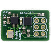
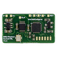
Description
There is a chance it may not be compatible with your display when going faster.
– Works with the GBA FP IPS screen
– Works with the FunnyPlaying laminated IPS GBA screen at speed 1.25x and below. At 1.5x, the screen fades to black as per a user report.
– Works with the GBC Q5 OSD display as per a user report
– Doesn’t work with the GBC FP Q5 screen or the GBC 2.45″ CGS display as per a user report
– Not recommended with the GBC FP IPS screen as per a user report, it’s glitchy.
– Not recommended with the GBA OneChip IPS screen as per a user report, it’s glitchy.
Using a faster clock may not work with all games or flash carts. Most genuine game cartridges should work. If you are using a GB flash cart that uses FRAM, if the game utilises double speed mode, there is a chance that your save data won’t be found if you increase the clock speed too much. GBA flash carts don’t seem to work when trying to go faster than 1x as they crash, going slower should work and the GBA only seems to allow 1.75x max. For the DMG, it will only respond to button presses if the game is querying the Dpad, e.g on the boot screen with the logo scrolling – it won’t respond to any changes.
If you have an AGB-001 or original DMG screen, when slowing down you will likely see some screen flicker. Installation requires a hot air gun to remove the existing crystal (for GBA/GBC, soldering iron is fine for DMG) and requires soldering. Consumes about 12mA of additional current and when the GBA/GBC/DMG is overclocked, it too will use 40-60mA more.
DMG Firmware available:
Standard – 0.85x, 1x, 1.25x, 1.5x
Pro (Safe) – 0.5x, 0.666x, 1x, 1.25x, 1.5x, 2x
Pro – 0.333x, 0.5x, 0.666x, 1x, 1.5x, 2x, 3x (Bad screen flicker will occur at 0.333x and LCD data corruption can occur at 3x)
GBC Firmware available:
Standard – 0.85x, 1x, 1.25x, 1.5x
Pro (Safe) – 0.333x, 0.5x, 0.666x, 1x, 1.25x, 1.5x
Pro – 0.333x, 0.5x, 0.666x, 1x, 1.25x, 1.5x, 2x (GBC only works with 2x max with genuine games)
GBA Firmware available:
Standard (new)- 0.333x, 0.5x, 0.666x, 1x, 1.25x, 1.5x, 1.75x
Standard (old) – 0.85x, 1x, 1.5x and 1.75x
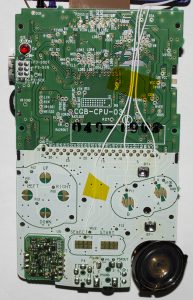
Installation (GBA)
1. Use a hot air gun to de-solder the existing crystal. Be careful not to remove any of the near by components.
2. Place the device as shown with some double sided tape or a little bit of blu-tack to insulate it from the GBA board and use the wiring below.
Device V+ to GBA SI
Device V- to GBA GND
Device CLK to GBA CK1
Device 1 to GBA TP2 (Select) or TP3 (Start)
Device 2 to GBA TP9 (L trigger)
Device 3 to GBA TP8 (R trigger)
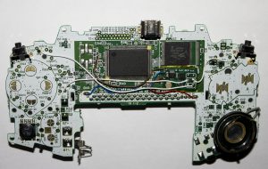
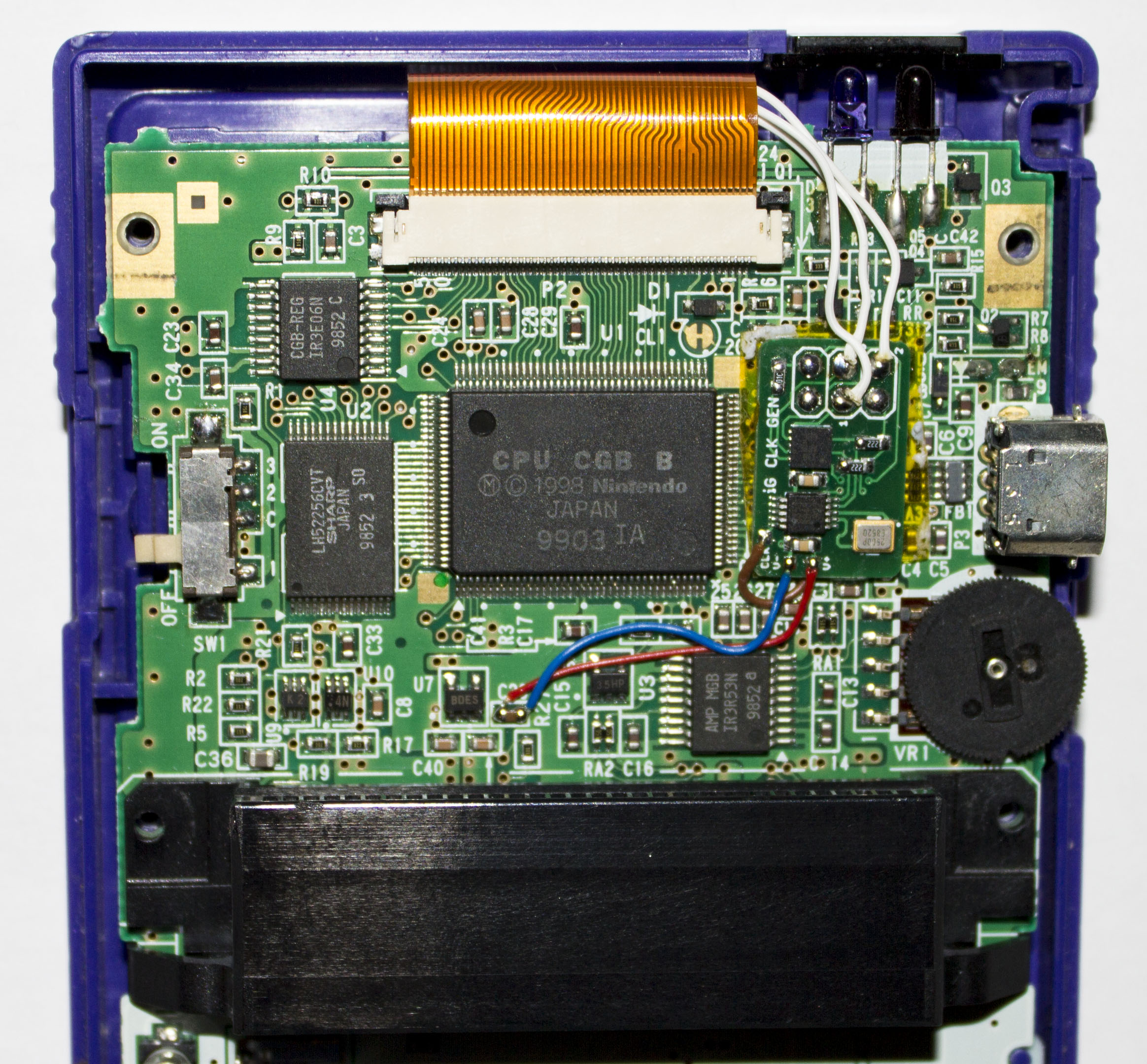
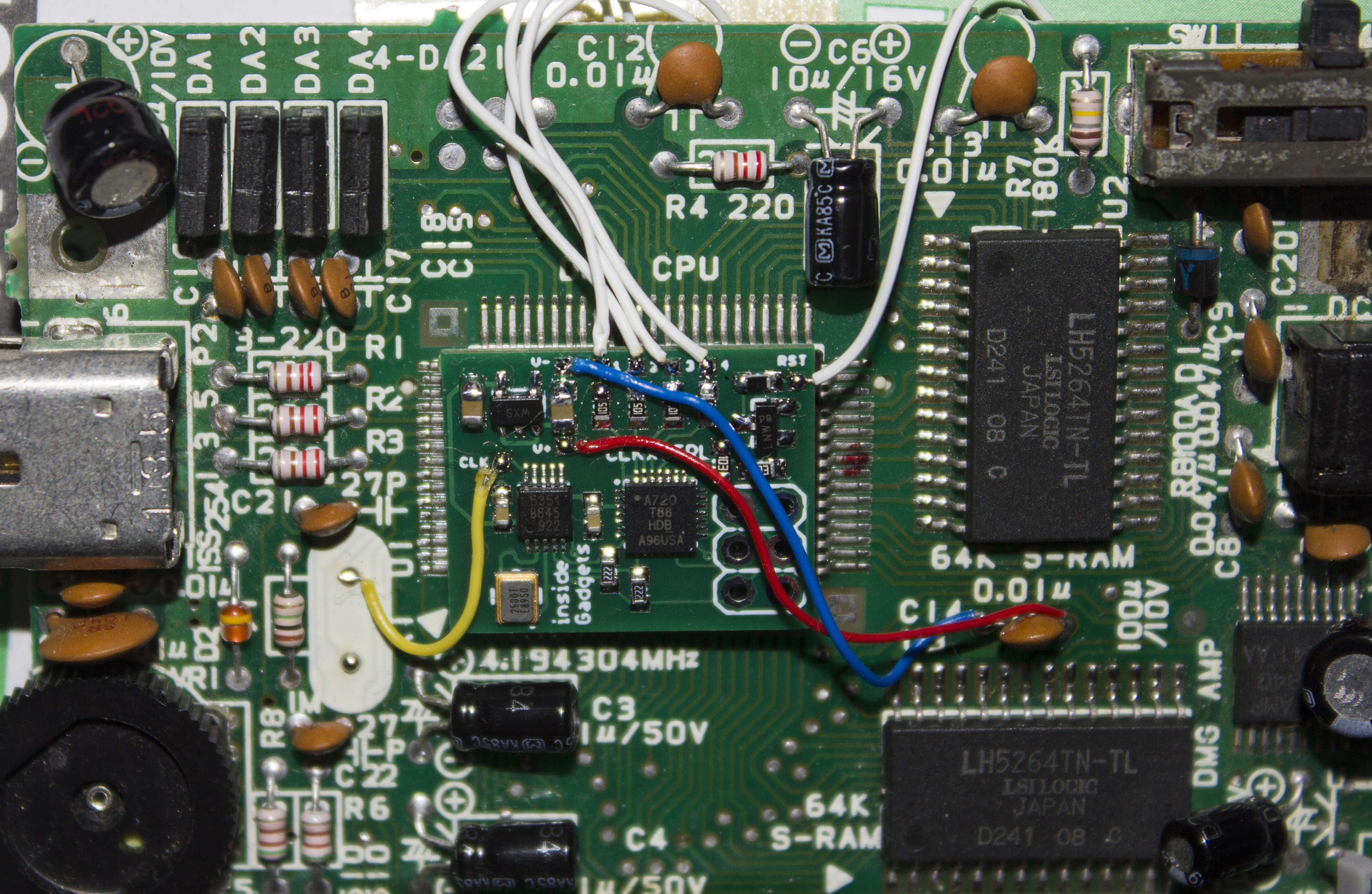
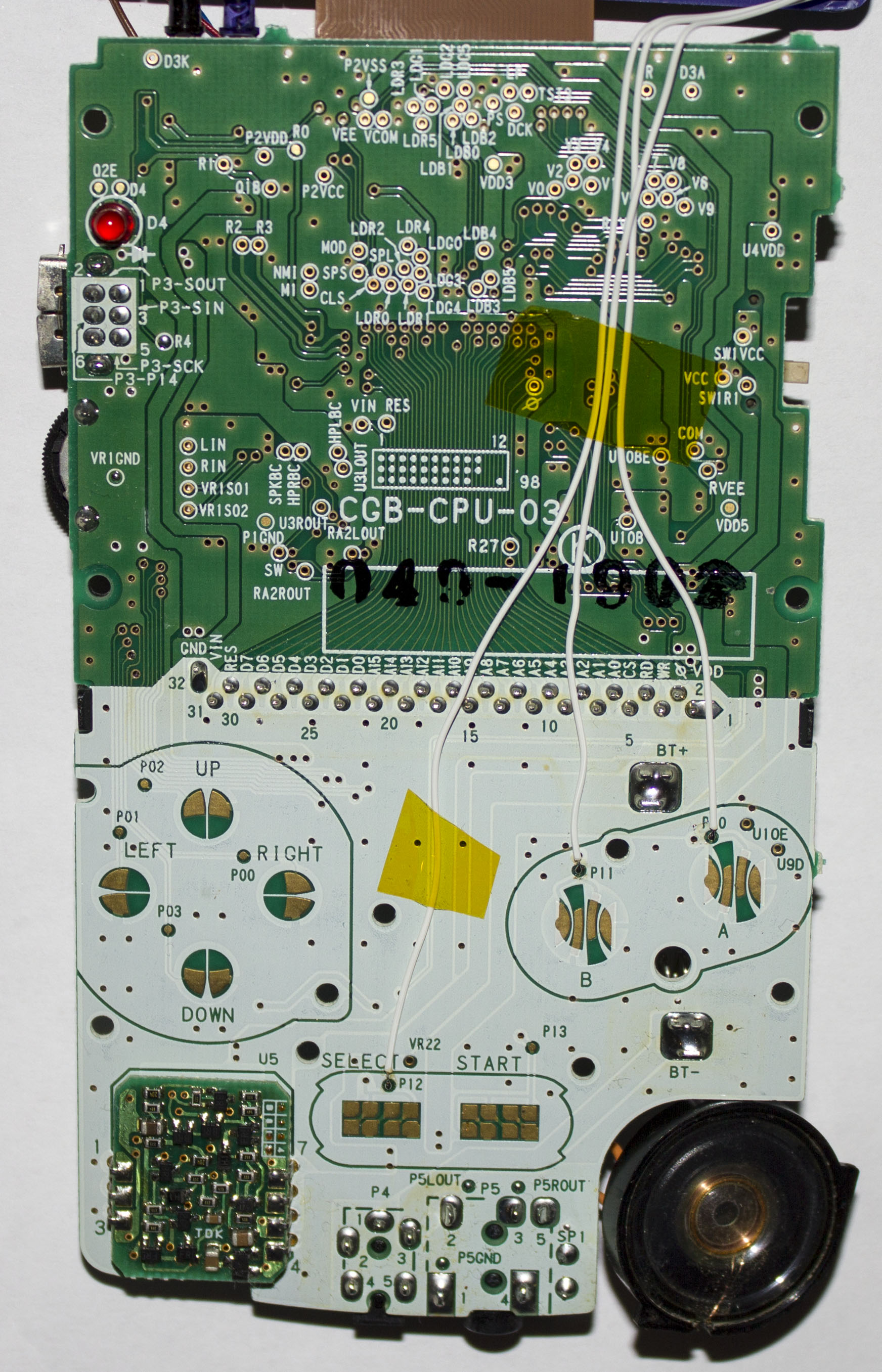
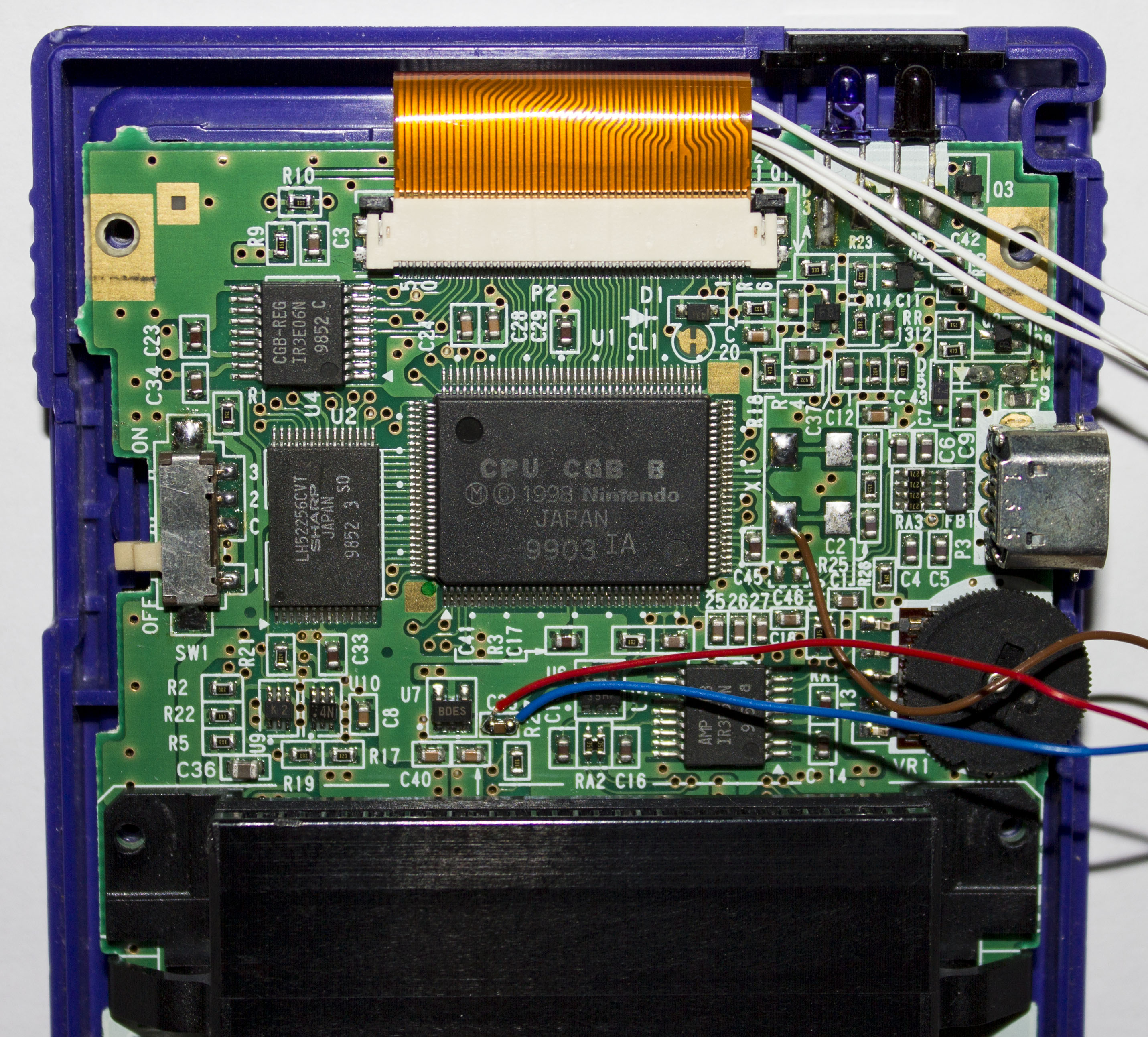
Installation (GBC)
1. Use a hot air gun to de-solder the existing crystal. Be careful not to remove any of the near by components.
2. Solder a wire to the P12 (Select), P11 (B) and P10 (A) pads. Route the wires upwards. You can use thin tape so they stay in place and don’t cover any screw holes.
3. Install the Gameboy colour PCB back into the shell. Solder a red and blue wire to the capacitor shown and another wire to the crystal pad. You can route the 3 button wires under the LCD ribbon cable for a neater solution (but be careful!).

4. Place the device as shown with some double sided tape or a little bit of blu-tack to insulate it from the GBA board. Trim the wires and solder them into place. You can install some kapton tape on the top to help hold it in place.

Device V+ to VCC pad as shown
Device V- to GND as shown
Device CLK to X1 pad as shown
Device 1 to P12 (Select)
Device 2 to P11 (B)
Device 3 to P10 (A)
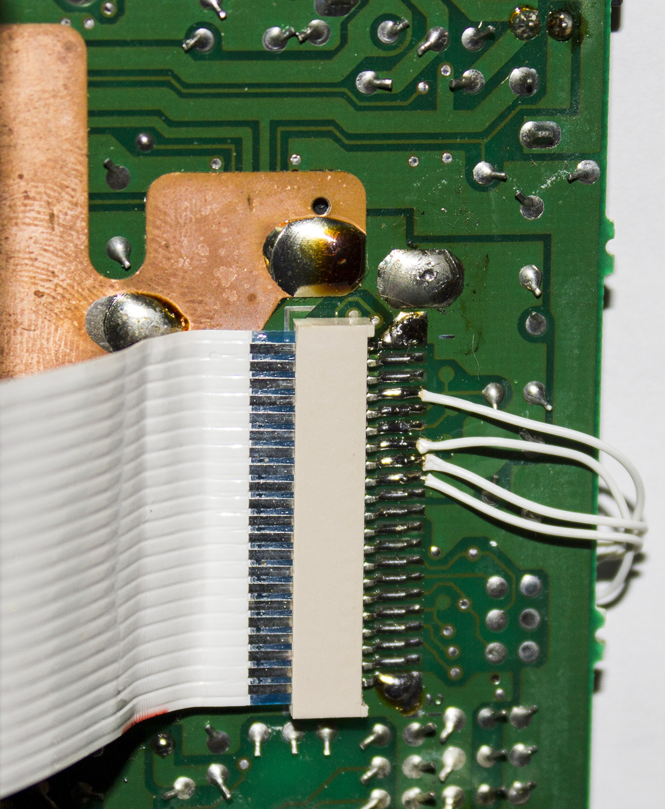
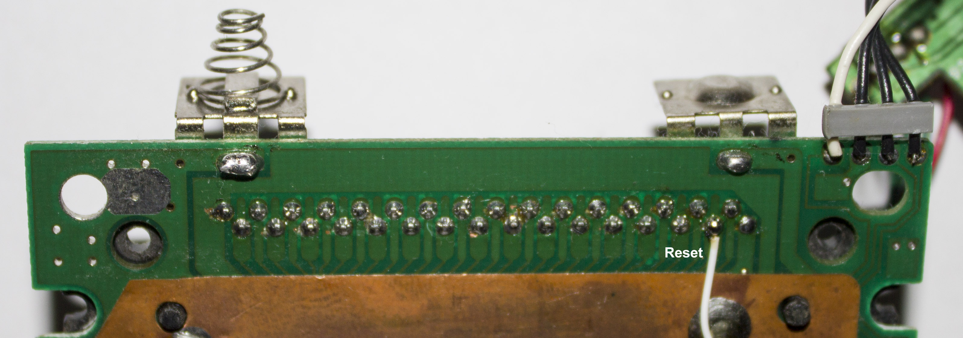
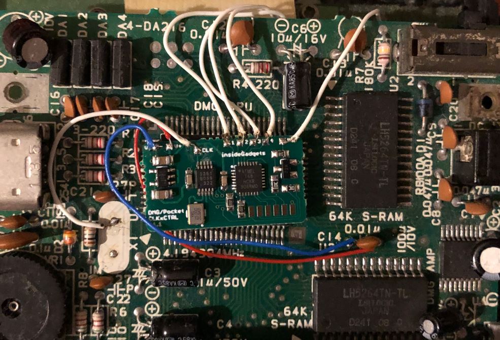
Installation (DMG)
1. Use soldering iron or hot air gun to de-solder the existing crystal. Be careful not to remove any of the near by components.
2. Solder a wire to the FFC connector on pins 4, 7, 8, 9.
3. Solder a wire to the reset pin (30) on the Gameboy connector.

3. Place the device on top of the CPU with some double sided tape or a little bit of blu-tack. Trim the wires and solder them into place. You can install some kapton tape on the top to help hold it in place.
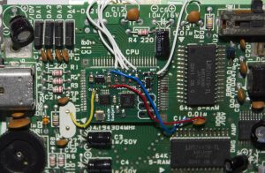

Device V+ to Capacitor +
Device V- to Capacitor GND
Device CLK to X0
Device pad 1 to FFC connector pin 7 (P12)
Device pad 2 to FFC connector pin 4 (P11)
Device pad 3 to FFC connector pin 8 (P10)
Device pad 4 to FFC connector pin 9 (P15)
Device RST pad to GB connector reset pin 30
Only logged in customers who have purchased this product may leave a review.

Reviews
There are no reviews yet.